Description:
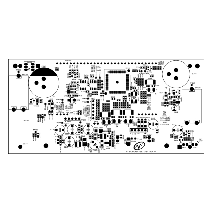
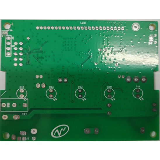
PCB Name:MTI‐3PEMLC‐65XX‐5‐180410
PCB Size :5.75x2.781 inch (146.05x70.64mm)
Layers :2
Board Thickness :1.6mm
Copper Foil Thickness :35um
Material :FR‐4 KB6160, 1oz, Cu, (Finish)
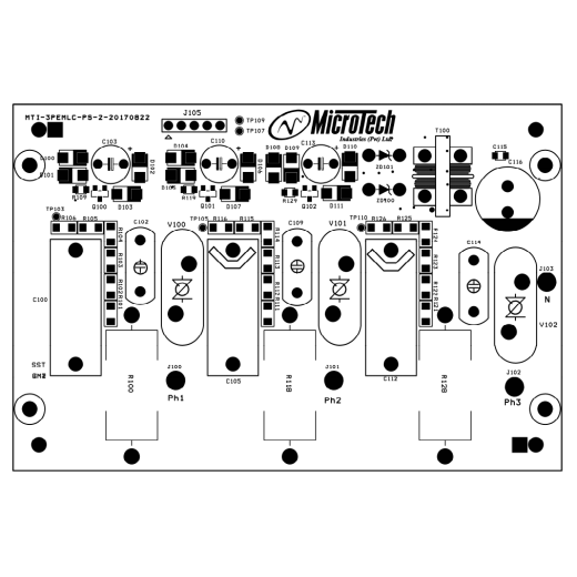
PCB Name MTI-3PEMLC-PS-2-20170822
PCB Size 4.25 inch x 2.85 inch
Layers 2
Number of PCBs in ONE Panel 6
Board Thickness 1.6mm
Copper Foil Thickness 35um
Material FR-4 KB6160, 1oz, Cu, (Finish)

Product Brochure:DOWNLOAD
Technical Parameters:
PCB design information | |
PCB name |
MTI‐3PEMLC‐65XX‐5‐180410 |
PCB size |
5.75x2.781 inch (146.05x70.64mm) |
Layers |
2 |
Number of PCBs in ONE panel |
6 |
Required PCB quantity |
------------) |
Board Thickness |
1.6mm |
Copper Foil Thickness |
35um |
Material |
FR‐4 KB6160, 1oz, Cu, (Finish) |
Finishing |
Lead free HASL |
Solder mask |
Green Both Side |
Solder Mask Type |
KGS‐6188G |
V-CUT |
NIL |
V-CUT Thickness |
yes |
Electrical Test / E. test |
Yes/Mark at board edge |
BOW and Twist |
≤0.75% |
Thermal Stress Test |
288°C/10 Sec |
Via hole |
NIL |
P.T.H. Thickness |
20um |
Silk Screen Layer |
White |
| Date code week/year Print on silk screen layer | Yes only this sample |
Component Marking Type |
M‐211(W) |
Tin/Lead Thickness |
≥1um |
Top and Bottom Registration |
+/‐ 3Mills |
Solder test |
≥95% with plum tin plating |
Hardness test |
6 H |
Cutting Slot |
Yes |
Technical Parameters:
PCB design information | |
PCB name |
MTI-3PEMLC-PS-2-20170822 |
PCB size |
4.25 inch x 2.85 inch |
Layers |
2 |
Number of PCBs in ONE panel |
6 |
Required PCB quantity |
--- (--- Panel) |
Board Thickness |
1.6mm |
Copper Foil Thickness |
35um |
Material |
FR‐4 KB6160, 1oz, Cu, (Finish) |
Finishing |
Lead free HASL |
Solder mask |
Green Both Side |
Solder Mask Type |
KGS‐6188G |
V-CUT |
yes |
V-CUT Thickness |
|
Electrical Test / E. test |
Yes/Mark at board edge |
BOW and Twist |
≤0.75% |
Thermal Stress Test |
288°C/10 Sec |
Via hole |
Plugged |
P.T.H. Thickness |
20um |
Silk Screen Layer |
White |
| Date code week/year Print on silk screen layer | Yes only this sample |
Component Marking Type |
M‐211(W) |
Tin/Lead Thickness |
≥1um |
Top and Bottom Registration |
+/‐ 3Mills |
Solder test |
≥95% with plum tin plating |
Hardness test |
6 H |
Cutting Slot |
Yes |
Our professional sales team are waiting for your consultation.